Friday, 30 November 2012

WEEK 14


Title of the project : Presentation during Engineering day


After day after day, week after week, month after month, after two semesters working for this final year project, this week is the last week before the project is presented at Gemilang Hall UNIKL BMI. The assessors for my project is Sir Azman and Sir Izwan 


some picture during presentation day


WEEK 13


Title of the project : Preparing the poster for presentation of Engineering day

        Before the Engineering day, the poster of presentation need to be prepared to give more easier to presenter to explain the project The poster should consist project description, objective, block diagram, methodology, result, and conclusion. During the presentation, student will have to explain all about the project by referring at the poster that already made. That is the use of the poster. Figure below shows my poster that will be used during the presentation day. 


Poster of the presentation during engineering day

WEEK 12


Title: Finishing the project


                The overall circuits that have be constructed before this need to compile in the hardware to complete the project. Figure below show the overall view of the project:

 all sources

side view 


Video explanation for four sources:


WEEK 11


 Title of the activity: Tabulating the result in the table   


            The results from the experiment for wind turbine and piezo film was record and tabulated in table. From the table it will be done in graph,  The output voltage that have be record will be proceed to do the analysis.

Table below shows the data from the experiment.

collector data for piezo films

graph for piezo films

collector data for wind turbine

graph for wind turbine

WEEK 10


Title:  Designing the casing of the project.

                This week I working on the selecting the material for the base and also the box to place all the circuit, battery and sources for the project. For avoiding problems occur when placing heavy wind turbine and large solar panel, L steel will be used to build the frame and thin layer of plywood to cover the L steel frame in this project. L steel will be cutting according to measurement by using grinder and for plywood saw will be used.For combine the L steel bolt and nut will be used. To touch up the project, lastly it will be spray with black color. Below is figure of material that be used:

pic of plywood

pic of L steel


WEEK 9


Title:  Source storage
                For source storage, I will be used A rechargeable battery, storage battery, or accumulator is a type of electrical battery. It comprises one or more electrochemical cells, and is a type of energy accumulator. It is known as a secondary cell because its electrochemical reactions are electrically reversible. Rechargeable batteries come in many different shapes and sizes, ranging from button cells to megawatt systems connected to stabilize an electrical distribution network. Several different combinations of chemicals are commonly used, including: lead–acid,nickel cadmium (NiCd), nickel metal hydride (NiMH), lithium ion (Li-ion), and lithium ion polymer (Li-ion polymer).
Rechargeable batteries have lower total cost of use and environmental impact than disposable batteries. Some rechargeable battery types are available in the same sizes as disposable types. Rechargeable batteries have higher initial cost, but can be recharged very cheaply and used many times.


top view rechargeable battery

front view rechargeable battery


WEEK 8


Title of activity: Design PCB board for charge controller circuit 


After the conformation on the circuit I start to design the circuit by using Dip trace software for the main circuit and for LCD circuit. After design I go to the printing shop to print the circuit layout to the transparent paper, after that I attach and stick the circuit layout on the transparent paper to the PCB board. Then I use iron to make the ink from the transparent paper stick to the PCB board.

After the ink properly sticks to the PCB board I need to check if any broken connection of the line circuit layout and need to repair by using marker. After satisfied with the connection I start to etching the PCB board. After etching I need to check the connection again to make sure no broken line and no connection are connect each other. After several of etching that satisfied me I start drill the hole by using driller to put the component on the circuit.

schematic diagram

PCB layout

drilling PCB for components

circuit charge controller


WEEK 7

Title of the activity: Designing the hump for piezo films


For the piezo films, its will be place at the hump. When the car go trough to the hump it will be pressing the piezo films. When it be press it will generates electricity. So I will design small scale of hump to place a piezo film to show how will the piezo films will be function and wasy for me to demo in the presentation.  I do by cutting half of milo tin to create the hump. Below is figure of hump for the piezo films.


hump with piezo


WEEK 6


Title of the activity: Designing the PCB layout for combination sources

For the combination circuit, it will need four inputs for four sources and will be one output before go to boost circuit. For this circuit, it just a simple circuit. So I don’t need to use software to draw the layout line. I only use permanent marker ink before do the etching. The component that is use  only t-block and diode. Below is figure of combination circuit:

top view of combination circuit


WEEK 5


Title of the activity : Designing the blade of the turbine.

            To design the blade to move the rotor of alternator to generated electricity, the light material will be used for wind turbine called “aluminium" was used. The criteria of using this aluminium is because it easy to design, cheap, and light. Figure below shows the picture of the blade.


blade be welding to the shaft


spraying the blade


WEEK 4


Title of activity: PCB board testing for boost circuit 


            For this week, the circuit board for boost circuit will be testing to know if the circuit can get the output as the simulation at the proteus software. The methods are when the supply from 9v from battery give supply to the boost circuit, the output should get almost two times higher from the voltage from battery. Figure below shows the PCB board of boost with the components.

top view of boost circuit


                                                            bottom view of boost circuit 


Video of testing boost circuit:


Thursday, 29 November 2012

WEEK 3

Title of the activity: Etching the circuit for the project       


           After the schematic diagram of the circuit was designed by using Diptrace software, the etching of the PCB board can be proceeded. The method that chosen to do the etching by using the iron. After the track of the circuit was printed on transparent plastic, the track of the circuit need to transfer to the PCB board. Hence, the plastic need to be ironed together with the PCB board. Then, for four more minutes, slowly move the iron around making sure to put a lot of pressure on the plastic, but not allowing the plastic to slide on the board. When done, let the board fully cool before moved it at all. This will allow the toner to adhere to the copper and prevent you from being burned.


          In a well-ventilated area with a fan, add 2-cups hydrogen peroxide to a plastic container. Gently pour in 1-cup Muriatic acid, to create the etching solution. Always wear goggles, gloves, and do not inhale the fumes. Do not use any metal containers, measuring cups, stainless steel sinks, or tools with this mixture as this mixture will aggressively etch metal. Acid safety, think “triple A”, for Always Add the Acid, it’s whatever is in the container that will end up splashing. This etching solution, while made with common chemicals, should command respect. It is dangerous to yourself and surroundings, treat it with respect. Ferric chloride is another common etching solution, it is not a safer solution to use, both are equally dangerous.

Below is picture of the process for etching:

Redo the copper line by using permanent marker


                                                             Etching the circuit board

WEEK 2


Designing the PCB layout for the boost circuit         


          Before this,the circuit of the project are constructed on breadboard. To proceed the project, the circuit need to soldered together on PCB board. The design of PCB layout was designed by using the proteus software. Figures below shows the layout of PCB for the boost receiver.

boost circuit layout


The layout for boost circuit for etching work


WEEK 1

During the last semester,I purchased all the hardware parts that I need to construct for the circuit. But I have a problem with the purchase because there are some components cannot be found in the store. The component such as piezo film is hard to find at Malaysia.So I must order the component online at the sparkfun.com.

Below is specification about piezo film:

Piezoelectric Film is an enabling transducer technology with unique capabilities. Piezo Film produces voltage in proportion to compressive or tensile mechanical stress or strain, making it an ideal dynamic strain gage. It makes a highly reliable, low-cost vibration sensor, accelerometer or dynamic switch element. Piezo Film is also ideally suited for high fidelity transducers operating throughout the high audio (>1kHz) and ultrasonic (up to 100MHz) ranges.


Piezo Film elements are offered in four variations:
·         Silver ink screen printed electrodes
·         Lamination for higher voltage output when bending
·         Flexible leads
·         Shielded sensors


Wednesday, 18 April 2012

Monday, 9 April 2012

Energy Harvester Circuit

This circuit will harvest energy from any small source such as a piezo electric buzzer element, speaker, solar cell.  It saves the energy to a 0.47 supper cap and boosts it to 3.3V using the Maxim chip.  The diode bridge is composted of low forward voltage BAT54 diodes.  The Max1675 has a quiescent current of less than 16uA. The zener protects the cap from over voltage.


Voltage Controlled Voltage Source Schematic

Monday, 26 March 2012

GREEN TECHNOLOGY PARKING SYSTEM

        As it week nine.I be asked to changed my fyp title to green technology and be do the project by group of two.My project basically about smart parking combine with green technology.For smart parking it makes easier for driver to find parking space.In the parking there will counting the parking space. When it show zero parking LCD will display 'FULL' so the driver will know that there is no parking in that place.We can survey the parking system by Visual Basic. This system will be placed at security place.
       This system will no use supply from MCB.This system will supply by the green technology.They are four types green technology that be used for supply to the system.We will be used Piezoelectric, kinetic, solar system and wind turbine.

Monday, 12 March 2012

HOW RFID WORKS


How does RFID work? A Radio-Frequency IDentification system has three parts:

A scanning antenna
A transceiver with a decoder to interpret the data
A transponder - the RFID tag - that has been programmed with information.
The scanning antenna puts out radio-frequency signals in a relatively short range. The RF radiation does two things:
It provides a means of communicating with the transponder (the RFID tag) AND
It provides the RFID tag with the energy to communicate (in the case of passive RFID tags).
This is an absolutely key part of the technology; RFID tags do not need to contain batteries, and can therefore remain usable for very long periods of time (maybe decades).
The scanning antennas can be permanently affixed to a surface; handheld antennas are also available. They can take whatever shape you need; for example, you could build them into a door frame to accept data from persons or objects passing through.

When an RFID tag passes through the field of the scanning antenna, it detects the activation signal from the antenna. That "wakes up" the RFID chip, and it transmits the information on its microchip to be picked up by the scanning antenna.

In addition, the RFID tag may be of one of two types. Active RFID tags have their own power source; the advantage of these tags is that the reader can be much farther away and still get the signal. Even though some of these devices are built to have up to a 10 year life span, they have limited life spans. Passive RFID tags, however, do not require batteries, and can be much smaller and have a virtually unlimited life span.

RFID tags can be read in a wide variety of circumstances, where barcodes or other optically read technologies are useless.

The tag need not be on the surface of the object (and is therefore not subject to wear)
The read time is typically less than 100 milliseconds
Large numbers of tags can be read at once rather than item by item.

Below is video tutorial, provided by Digi-Key and Texas Instruments, will answer the questions What is RFID and how does it work? and examine how the frequency of operation affects the characteristics of the system and in turn influences the choice of application.

                         RFID Technology and Applications


USB DATA ACQUISITION WITH PIC18

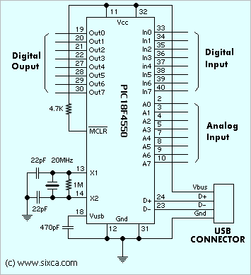
This project is simple and small component count USB data acquisition or USB DAQ. The main core of USB device is PIC18F4550 .The firmware for PIC modified from Microchip CDC library.

Specifications

- 8 Digital output
- 8 Digital input
- 8 Analog output
- No external power required
- Simple ASCII command 
- 3 command to communicate PC with PIC 


                                                                    Figure  Schematic


Project Hardware


The analog signal from the microphone was amplified using an op-amp and then digitized using the 16C745's analog-to-digital feature.  If you are reproducing this project, I would recommend putting in a filter to remove the frequencies higher than the microprocessor's sampling rate.  The digital data was buffered in the microprocessor and then set to the host computer over the USB connection.  Since 'interrupt' method of transfer only allows 8 bytes of data transfered every 10ms, this limited the amount of data that could be transfered.
The following circuit connects the PIC to the usb cable. It is designed to be powered off the USB cable. The 6 MHz clock controls the internal oscillator.

The 'reset' switch, causes a reset condition which should cause most of the special registers to clear and the program to start again.

The value of R1 is not critical since it is only used as a pull-up for the MCLR (master clear) pin. The R2 resister is required by the USB specification and should be 1.5 kOhms. The capacitor C3, is not critical and simply stabilizes the Vusb pin voltage. The values of the capacitors, C1 and C2 can be in a range specified in the 16C745 specification (15pf - 69 pf) and may depend on the crystal that you use.

Check that USB power and ground connections are correct before connecting the chip. It is easy to get turn around between the cable pinout and the socket pin out.


Circuit Diagram showing USB connections
The following circuit is used to power the electret microphone and then amplify the signal. The output signal is connected to one of the analog pins of the 16C745, we used pin 2, corresponding to AN0 (analog pin 0).


Microphone Powering Circuit


SD MEMORY CARD INTERFACE


SD memory cards, especially the ones under 1GB are cheap, relatively easy to interface and provide vast amounts of memory for imbedded control.

This device lets reading to sd cards through your serial port. Communication is in ASCII so you just need a terminal program to access it. 

                                          The Hardware

SD sockets are available from SparkFun Electronics. The socket needs to be surface mounted so it was placed on the foil side of the single sided board. The connections are close to 0.1 inch centers, so the layout was not difficult.

The PIC16F819 was chosen for its hardware support for SPI. (SD cards will usually work through an SPI interface) Running at 20Mhz, the SPI port clocks data at 5Mhz, and the serial communication is able to run at 115200 baud in software.
A quick look at the schematic shows one way to interface the 5 volt PIC to the 3.3 volt SD card. A red LED drops the 5 volt supply by about 1.8 volts to feed about 3.2 volts into the card. This is within the operating range.

Signals from the PIC go through a 1k/2k voltage divider to feed signals to the card. Signals back from the card feeding SDI input are a problem because the PIC uses schmit-trigger inputs in SPI mode requiring 3.5 volts for the high level. The circuit provides a 0.6 volt shift so the output of the card back to the PIC ranges from 0.6 to 3.8 volts. Cheesy, but it works.

The Software

The main issue with the software is configuring the SPI port. After a lot of diddling around, the proper setup seems to be: SMP=1, CLE=1, and CKP=1. See the software listing for the complete setups of SSPSTAT and SSPCON registers in sspinit. The routine that writes to the card also reads it, since, in SPI, read and write are simultaneous operations.

Once connected to a terminal program (115200 baud, 1 stop bit, no parity, no handshaking), the following commands are available:
CommandFunction
S
Select Card
D
Deselect Card
Zddd
Send ddd bytes of clocks
W xx xx xx xx xx ...
Send series of (hex) bytes
Cdd ddddd
Send command dd containing
address 512*ddddd
Xddd xx
Send ddd bytes of (hex) value xx
Rddddd
Read ddddd bytes from card
Ctrl-CResend last command
ddd = decimal value, xx = hex value
Commands can be combined on a single line, for example...
C17 2 R520
Command 17 (read sector) at address 1024 (start of sector 2) followed by read back 520 bytes.
C0 0 R2 C1 0 R2 C1 0 R2
Setup board for SPI, read status, init board, check status, check init, read status.
Note that the C command generates an effective 'sector address' by multiplying by 512. It also generates the mandatory 95 (hex) CRC that is only required for Command 0 to put it in SPI mode. After that, the CRC is not required for any other commend.
If you want to issue a command the needs specific parameters other than a sector address, you need to use the W command with everything in hexadecimal.
Eventually, this device is to be made into an SD card programmer/reader. For now, its a way to probe the operation of various manufacturers cards.


Wednesday, 22 February 2012

THING TO DO WEEK 6


SMART RFID ATTENDANCE

        Basically my project is about Interactive attendance capture by using RFID system.So now I must change the project to smart RFID attendance.This new idea can save some cost and make it simple and portable.  By this we don't need to use wireless system to sent data and receive data from the PC.The data only save in memory card and will insert into RFID circuit.Data will be read when RFID scanning student ID. 
       So my task this week to do research how to make smart RFID attendance.Study more more about RFID with memory card. 

Monday, 13 February 2012

PIC 16 VS PIC 18

The 16F is 14 bit, and the 18F is 16 bit, this allows the 18F series to have a larger instruction set - the 18F has an instruction set that's optimised for use with C, and MicroChip even provide a free C compiler for it. Essentially it's a higher end version of the 16F, and runs faster as well, with an internal PLL that can run four times faster than the external crystal.

If you're starting PIC programming, the 16F are a good place to start. It's a fairly easy progression to the 18F.

Pic16F is Slow. If you want to make blinking lights it is fine. For Pic18F, if you are gonna use a pic you might as well start using the Pic18 instead, they are just as cheap as the Pic16 and generally offer better. 

If you must choose PIC then it better to choose the PIC18. If you must use PIC16 then use can use any language you want, suitable for simple language like something that is easy and quick.

PIC18F2455/2550/4455/4550


OVERVIEW

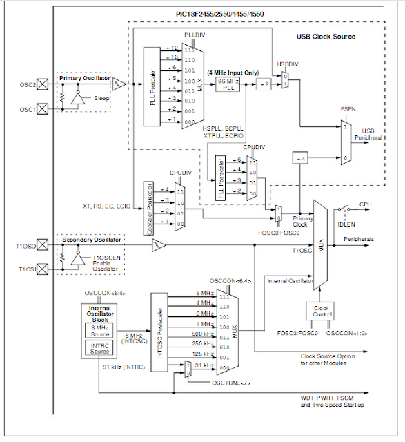
Devices in the PIC18F2455/2550/4455/4550 family incorporate a different oscillator and microcontrollerclock system than previous PIC18F devices. The addition of the USB module, with its unique requirements for a stable clock source, make it necessary to provide a separate clock source that is compliant with both USB low-speed and full-speed specifications.To accommodate these requirements, PIC18F2455/ 2550/4455/4550 devices include a new clock branch toprovide a 48 MHz clock for full-speed USB operation.Since it is driven from the primary clock source, an additional system of prescalers and postscalers has been added to accommodate a wide range of oscillator frequencies. An overview of the oscillator structure is shown in figure below.Other oscillator features used in PIC18 enhanced microcontrollers, such as the internal oscillator block and clock switching.The pins for PIC 16 and PIC 18 are 97% identical between the two chips.

PIC18F2455/2550/4455/4550 CLOCK DIAGRAM