Friday, 30 November 2012

WEEK 7

Title of the activity: Designing the hump for piezo films


For the piezo films, its will be place at the hump. When the car go trough to the hump it will be pressing the piezo films. When it be press it will generates electricity. So I will design small scale of hump to place a piezo film to show how will the piezo films will be function and wasy for me to demo in the presentation.  I do by cutting half of milo tin to create the hump. Below is figure of hump for the piezo films.


hump with piezo


WEEK 6


Title of the activity: Designing the PCB layout for combination sources

For the combination circuit, it will need four inputs for four sources and will be one output before go to boost circuit. For this circuit, it just a simple circuit. So I don’t need to use software to draw the layout line. I only use permanent marker ink before do the etching. The component that is use  only t-block and diode. Below is figure of combination circuit:

top view of combination circuit


WEEK 5


Title of the activity : Designing the blade of the turbine.

            To design the blade to move the rotor of alternator to generated electricity, the light material will be used for wind turbine called “aluminium" was used. The criteria of using this aluminium is because it easy to design, cheap, and light. Figure below shows the picture of the blade.


blade be welding to the shaft


spraying the blade


WEEK 4


Title of activity: PCB board testing for boost circuit 


            For this week, the circuit board for boost circuit will be testing to know if the circuit can get the output as the simulation at the proteus software. The methods are when the supply from 9v from battery give supply to the boost circuit, the output should get almost two times higher from the voltage from battery. Figure below shows the PCB board of boost with the components.

top view of boost circuit


                                                            bottom view of boost circuit 


Video of testing boost circuit:


Thursday, 29 November 2012

WEEK 3

Title of the activity: Etching the circuit for the project       


           After the schematic diagram of the circuit was designed by using Diptrace software, the etching of the PCB board can be proceeded. The method that chosen to do the etching by using the iron. After the track of the circuit was printed on transparent plastic, the track of the circuit need to transfer to the PCB board. Hence, the plastic need to be ironed together with the PCB board. Then, for four more minutes, slowly move the iron around making sure to put a lot of pressure on the plastic, but not allowing the plastic to slide on the board. When done, let the board fully cool before moved it at all. This will allow the toner to adhere to the copper and prevent you from being burned.


          In a well-ventilated area with a fan, add 2-cups hydrogen peroxide to a plastic container. Gently pour in 1-cup Muriatic acid, to create the etching solution. Always wear goggles, gloves, and do not inhale the fumes. Do not use any metal containers, measuring cups, stainless steel sinks, or tools with this mixture as this mixture will aggressively etch metal. Acid safety, think “triple A”, for Always Add the Acid, it’s whatever is in the container that will end up splashing. This etching solution, while made with common chemicals, should command respect. It is dangerous to yourself and surroundings, treat it with respect. Ferric chloride is another common etching solution, it is not a safer solution to use, both are equally dangerous.

Below is picture of the process for etching:

Redo the copper line by using permanent marker


                                                             Etching the circuit board

WEEK 2


Designing the PCB layout for the boost circuit         


          Before this,the circuit of the project are constructed on breadboard. To proceed the project, the circuit need to soldered together on PCB board. The design of PCB layout was designed by using the proteus software. Figures below shows the layout of PCB for the boost receiver.

boost circuit layout


The layout for boost circuit for etching work


WEEK 1

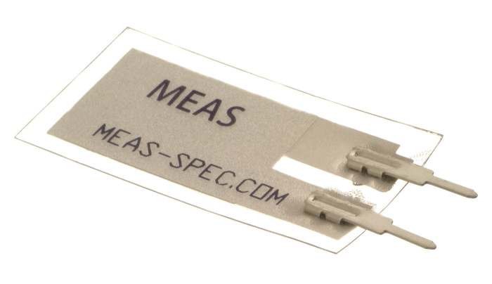
During the last semester,I purchased all the hardware parts that I need to construct for the circuit. But I have a problem with the purchase because there are some components cannot be found in the store. The component such as piezo film is hard to find at Malaysia.So I must order the component online at the sparkfun.com.

Below is specification about piezo film:

Piezoelectric Film is an enabling transducer technology with unique capabilities. Piezo Film produces voltage in proportion to compressive or tensile mechanical stress or strain, making it an ideal dynamic strain gage. It makes a highly reliable, low-cost vibration sensor, accelerometer or dynamic switch element. Piezo Film is also ideally suited for high fidelity transducers operating throughout the high audio (>1kHz) and ultrasonic (up to 100MHz) ranges.


Piezo Film elements are offered in four variations:
·         Silver ink screen printed electrodes
·         Lamination for higher voltage output when bending
·         Flexible leads
·         Shielded sensors